

We have 3 types of non-insulated DC to DC convertes: Buck, Boost and Buck-Boost configurations.
(Take It from http://www.electronoobs.com/eng_circuitos_tut10.php )
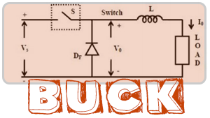
BUCK
1.0 DC to DC buck converter
A buck converter (step-down converter) is a DC-to-DC power converter which steps down voltage (while stepping up current) from its input (supply) to its output (load). It is a class of switched-mode power supply (SMPS) typically containing at least two semiconductors (a diode and a transistor, although modern buck converters frequently replace the diode with a second transistor used for synchronous rectification) and at least one energy storage element, a capacitor, inductor, or the two in combination. To reduce voltage ripple, filters made of capacitors (sometimes in combination with inductors) are normally added to such a converter's output (load-side filter) and input (supply-side filter).
In this tutorial we will learn how to build and how a DC to DC buck converter works. The circuit is very basic using just one diode, an inductor and a capacitor. The switch will be a MOSFET transistor and to create the PWM signal we will use a 555 timer in the PWM configuration, boost adjustable controller or one Arduino NANO. But first let's study a little bit of theory. We have the Buck converter circuit in the next figure where we can see the switch, inductor and capacitor and of course we add a load to the output.
2.0 Buck converter theory
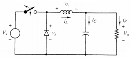
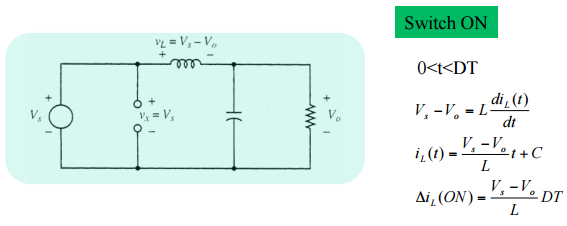
Ok, so we have the next circuit. In order to study how it works, we will divide it in two stages. The ON and OFF stages. In the ON part, the switch is closed as we can see in the next figure where the diode is open becasue the cathode voltage is higher than the anode. When the switch is first closed (on-state), the current will begin to increase, and the inductor will produce an opposing voltage across its terminals in response to the changing current. This voltage drop counteracts the voltage of the source and therefore reduces the net voltage across the load. Over time, the rate of change of current decreases, and the voltage across the inductor also then decreases, increasing the voltage at the load. During this time, the inductor stores energy in the form of a magnetic field. If the switch is opened while the current is still changing, then there will always be a voltage drop across the inductor, so the net voltage at the load will always be less than the input voltage source. When the switch is ON the inductor will charge up and the voltage on the inductor will be the difference between the output and the input. But we also know that the inductor voltage is the inductance L multiplied by the inductor current derivate. As we can see in the next figure we obtain the ON current through the inductor.
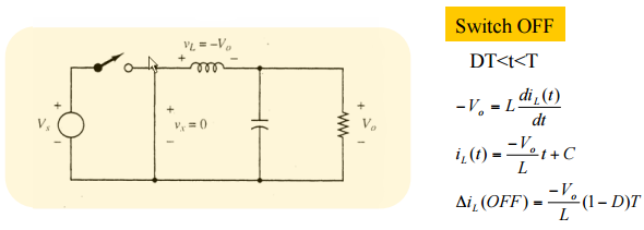
When the switch is opened again (off-state), the voltage source will be removed from the circuit, and the current will decrease. The decreasing current will produce a voltage drop across the inductor (opposite to the drop at on-state), and now the inductor becomes a Current Source. The stored energy in the inductor's magnetic field supports the current flow through the load. This current, flowing while the input voltage source is disconnected, when concatenated with the current flowing during on-state, totals to current greater than the average input current (being zero during off-state). The "increase" in average current makes up for the reduction in voltage, and ideally preserves the power provided to the load. During the off-state, the inductor is discharging its stored energy into the rest of the circuit. If the switch is closed again before the inductor fully discharges (on-state), the voltage at the load will always be greater than zero.
In this case the voltage across the inductor is the output voltage. So once again using the next figure formulas we obtain the current of the OFF part.
Ok, now if we want to obtain the output depending on the input and the duty cycle of the PWM all we have to do is to make the sum of the On and Off current equal to 0. That means that the On current is equal to the Off current. So the will give us:
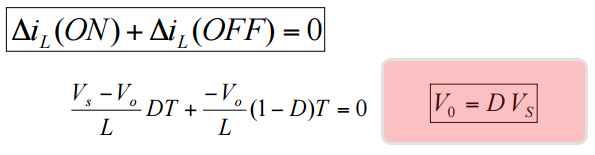
So we've obtain that the output is the input multiplied by the duty cycle. The duty cycle of the PWM can have values between 0 and 1. So te only posible output will be equal or lower than the input. That's why this configuration is called step down converter.
3.0 Buck converter Arduino NANO
Sincerely, this circuit has no other sense but to learn. The Arduino NANO already has a 5V linear voltage regulator that will lower the efficiency of the circuit. So the main goal is to learn how the circuit, the feedback and the PWM signal work in order to achive the desired output.
3.1 NO FeedBack
Arduino NANO
P-MOS: IRF4905
Schottky Diodes
100uF cap
150uH coil
S8050 NPN
Resistors
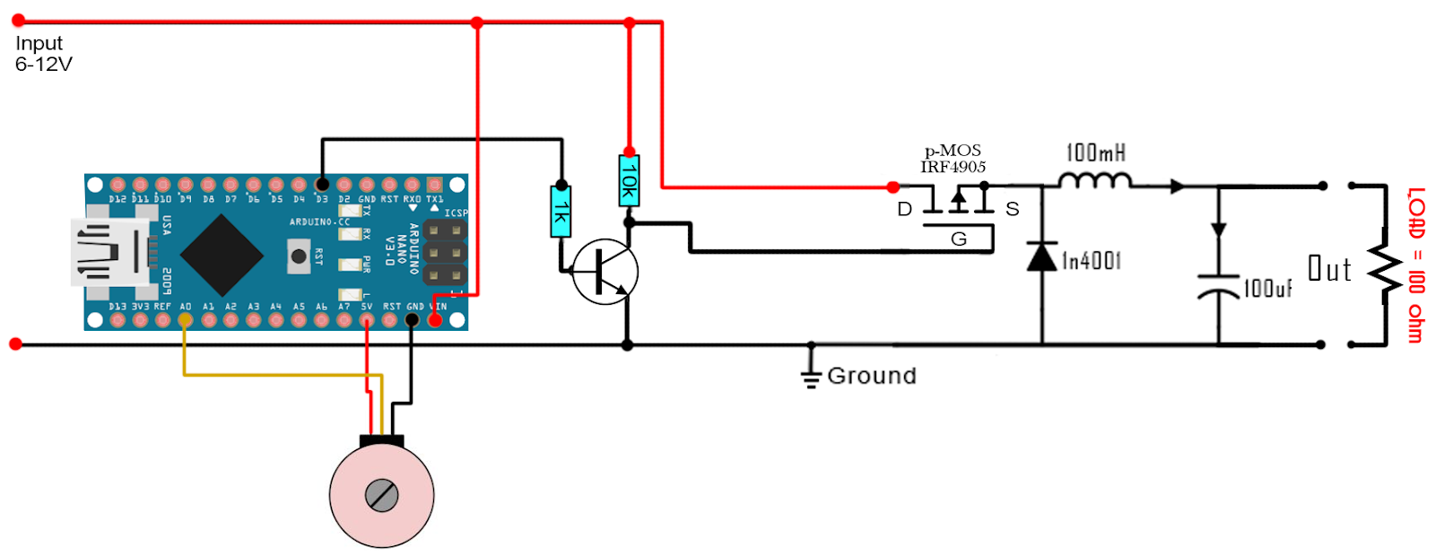
As you can see in the schematic above we have a potentiometer connected to the analog input A0. With this potentiometer we will choose the output value between 1 and 12 volts since the maximum input voltage in this case is 12V. With the Arduino's ADC we will read a value between 0 and 1024, next, in the code we map that value from 1 to 244 which are the values used with the analogWrite function of the arduino. With this we will apply a PWM signal on pin D3 where 1 is the lowest duty cycle and 244 the maximum. Since the arduino digital value is 5V we add a small BJT driver using one S8050 NPN and two resitors of 10k and 1k. The output of this driver is connected to the gate of the IRF4905 P-MOSFET.
Connect everything as in the schematic above and upload the next code to your Arduino and start moving the potentiometer. Observe the otput on the oscilloscope.
NO FEEDBACK code here
BUCK_NO_FEEDBACK.ino
Código: Seleccionar todo
/*
 * This is an example code for a BUCK converter circuit made with arduino
 * I've used arduino NANO. We have to set the timer of the PWM on pin D3
 * No feedback is connected here
 * Subscribe: http://www.youtube.com/c/electronoobs
 * webpage: http://www.electronoobs.com/eng_circuitos_tut10.php
 */

int potentiometer = A0; //From the main potentiometer
int PWM = 3;


void setup() {
  pinMode(potentiometer, INPUT);
  pinMode(PWM, OUTPUT);
  TCCR2B = TCCR2B & B11111000 | B00000001;    // pin 3 and 11 PWM frequency of 31372.55 Hz
}

void loop() {

  float voltage = analogRead(potentiometer);
  int VALUE = map(voltage,0,1024,0,254);
  analogWrite(PWM,VALUE);

}
3.2 FeedBack
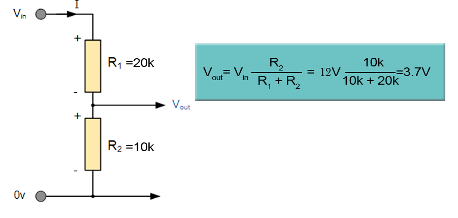
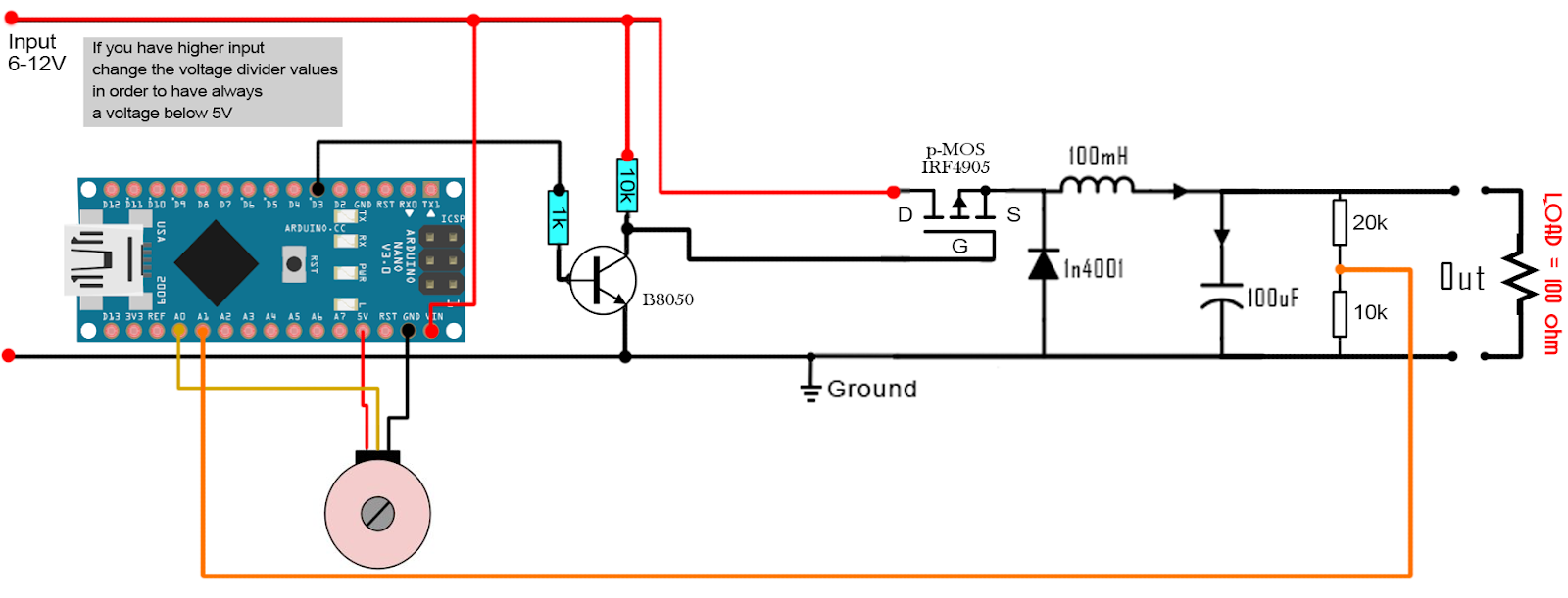
Let's add the feedback to our circuit. As you can see in the schematic below we have a potentiometer connected to the analog input A0 as before. With this potentiometer we will choose the desired output value between 1 and 12 volts since the maximum input voltage in this case is 12V. At the output of the circuit we have nowa voltage divider that will lower the voltage from 12V to under 5 volts because that's the maximum input voltage of the Arduino ADCs. Check the formula below to understand how the voltage divider works. If you apply a higher voltage to the input than 12V you should change the values of R1 and R2 in order to always have a voltage below 5V for the ADC.
In the code we compare this two voltages and increase or decrease the PWM width in order to keep the output constant. Just copy and upload the next code to the Arduino for this example.
Connect everything as in the schematic above and upload the next code to your Arduino and start moving the potentiometer. Observe the otput on the oscilloscope.
FEEDBACK code here
BUCK_FEEDBACK.ino
Código: Seleccionar todo
/* This is an example code for a BUCK converter circuit made with arduino
 * I've used arduino NANO. We have to set the timer of the PWM on pin D3
 * The feedback is connected to A1 and we set the desired voltage with a
 * potnetiometer connected to A0.
 *
 * Subscribe: http://www.youtube.com/c/electronoobs
 * webpage: http://www.electronoobs.com/eng_circuitos_tut10.php
 */


int potentiometer = A0;
int feedback = A1;
int PWM = 3;
int pwm = 0;

void setup() {
  pinMode(potentiometer, INPUT);
  pinMode(feedback, INPUT);
  pinMode(PWM, OUTPUT);
  TCCR2B = TCCR2B & B11111000 | B00000001;    // pin 3 and 11 PWM frequency of 31372.55 Hz
}

void loop() {
  float voltage = analogRead(potentiometer);
  float output  = analogRead(feedback);

  if (voltage > output)
   {
    pwm = pwm-1;
    pwm = constrain(pwm, 1, 254);
   }

  if (voltage < output)
   {
    pwm = pwm+1;
    pwm = constrain(pwm, 1, 254);
   }

   analogWrite(PWM,pwm);
}
With this component we have feedback and the output will stay the same using different loads. Just make the connections, add the input capacitor to have a steady input and you're done.
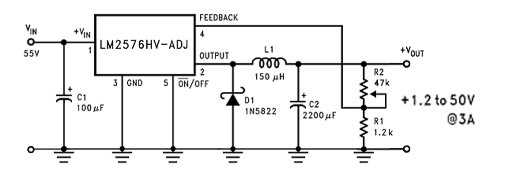
The input could be in range of 5 to 55 volts. Don't apply higher voltage or you could burn LM2576T-ADJ component. In this case we need no external switch since the LM2576T-ADJ already has it inside it. With the feedback pin connected to the output voltage divider, the LM2576T-ADJ will change the width of the pulse depending of the output in order to keep it constant. In this case use a Schottky Barrier Rectifier diode because it has a low forward voltage. This diode will live the current flow when the switch is open
3.0 Buck converter circuit 555 timer
This 555 configuration will create a PWM signatl and apply that signal to the MOSFET gate. The circuit works ok but it has a big problem. The output will change if we change the output load because the circuit has no feedback. Ok so we will use the next schematic for our buck converter. To create the PWM signal we will use the 555 timer with the PWM configuration. With the P1 potentiometer we can change the duty cycle of the PWM signal, and at the same time the output value. For the MOSFET you could use the IRF4905 P channel mosfet. You could always try different inductance values for the inductor and see the results.
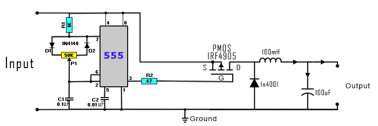
The input could be in range of 5 to 15 volts. Don't apply higher voltage or you could burn the 555 timer. Connect the PWM (pin 3 of the 555 timer) to the MOSFET (switch) gate. Add an output load and test the circuit. You could obtain output valuew between 1V and 15V.